February 6, 2013, 3:07 pm
A couple of weeks ago I introduced PCBmodE, software I wrote for creating functional and artistic PCBs. Other than the artsy bit, the unique feature of PCBmodE is that the board is completely generated from information stored in JSON files, so it's completely revision-controlled, cross-platform (software written in Python), and portable. I like to say that "my board is compiling" while on reddit ;) Its native graphical representation is SVG with a post-processor for generating "extended Gerber" files for manufacturing.
Since the last update, I've added auto-generated measurement arrows to indicate the board's dimensions, a layer index, and the ability to add information to the documentation layer. I've also rearranged the structure of the project and made it more presentable in preparation to releasing it. Here's how 'pieceof' revision A looks like as sent to the PCB house:
![]() |
| A PNG of the SVG with all layers included |
![]() |
| View of Gerbers using 'gerbv' (gerbv's bitmap export isn't great; it all looks very smooth and aligned) |
After communicating with a few PCB manufacturers I finally sent out the board for fabrication with Eurocircuits, who have a PCB viewer as part of the ordering process -- very useful for me. I ordered ten pieces that should be here within seven working days!
↧
February 12, 2013, 12:26 am
Below is a an image from the PCB manufacturer of the board's files after they have processed them. I noticed a couple of manual changes that they have made that affect how the board looks; one example is the outline of the Open Source Hardware logo -- it was supposed to go all the way round. I'll compare everything when the board arrives by the end of the week. Exciting!
![]() |
| The image supplied to me is at this low resolution |
↧
↧
February 12, 2013, 9:57 am
I'm happy to announce that the code for PCBmodE has just been released under the Apache License Version 2.0! Please read the overview, and let me know what you think. Also feel free to comment on the code, raise issues, and edit the wiki.
By the way, if you don't have a bitbucket account and I send you an invitation I get some minor perks, so...
↧
February 16, 2013, 4:32 am
I've just pushed an update to PCBmodE in the development branch. It adds support for drilling, and removes the pad files that were included in earlier designs.
![]() |
| The 'drills' design (a PNG taken of the SVG PCBmodE produces). You can't quite see it, but each drill has a tiny diameter text so it's only visible when you zoom in. |
For the drills, there's a new -e / --make-excellon option that will produce an Excellon file. While it displays well with 'gerbv' I still need to test that I got everything right, and that's why the feature is still in the 'development' branch. The Drill index is added automatically if you ask the tool to do so. You can also choose whether you want soldermask around the drill and so on. Here's how it looks in 'gerbv':
![]() |
| A view from 'gerbv'; the Excellon data is in yellow. |
You can see the input JSON file that created the board above here.
Regarding the removal of pad files, my initial thought was that pads could be reused between part definitions and therefore it would be useful to have them as standalone files. However, based on my board design experience, it's rather rare to have the exact same landing patterns across parts, even for boards with dozens of components. For PCBmodE's more artistic designs, some of the pads would be unique anyway, so are not that reusable. Finally, it makes more conceptual sense for the entire footprint definition to be enclosed in a single file. So, from now on, pad prototypes are defined inside of the part definition.
↧
February 18, 2013, 1:42 pm
I've just pushed an update to the development branch of PCBmodE here. This update includes support for multiple layers, although only top and bottom are tested for now. (Everything is set to define more than two layers, but I haven't constructed a board to test it, so it will be officially supported at a later time.) I also added the 'both' board for testing the two layers. Here's how it looks:
![]() |
| The 'both' board |
You can get the SVG for 'both' from here.And here's a snapshot from 'gerbv':
![]() |
| The 'both' board as seen in the 'gerbv' viewer |
Notice that I have also changed the colour scheme, which is defined like CSS in a JSON file, so it's easy to change and manipulate. Here's how 'pieceof' looks like in this new scheme. ![]() |
| The 'pieceof' board in the new colour scheme |
You can download the SVG of 'pieceof' from here. Ten pieces of 'pieceof' should arrive tomorrow or the day after!
↧
↧
February 19, 2013, 9:01 am
The 'pieceof' board, the first to be manufactured using PCBmodE, has arrived this morning! Here are a few pictures before a more in-depth analysis of the results.![]() |
| With back-lighting we can see the features better |
![]() |
| The terminals in the edge are for clips or alligators |
![]() |
| The LED arrangement with a few components |
↧
February 23, 2013, 4:58 am
I've just pushed an update to PCBmodE's development branch. This one includes everything that's needed to support both surface layers (that is, 'top' and 'bottom'), but much more significantly, a restructuring of the SVG layers for both footprints and boards.
You wouldn't notice the difference unless you've opened up the SVGs PCBmodE produces in a text editor. It was a bit of a mess, and now it's better. What this restructuring will allow is easier maintenance and addition of features. I've also changed the structure of footprint definition so it's more consistent with how board features are defined. Again, you wouldn't notice anything unless you've edited them; all the footprints in the new push have been refactored to the new style.
As a test for the new features, I've used the 'drills' design. Here is it in PNG and as seen in 'gerbv'. You can download the SVG here -- open it up with Inkscape and press CONTROL-SHIFT-L to turn the layers on and off.
Next on my todo list is adding support for vias and then support copper pours. Also, there are a few areas where processing time can improve.
↧
February 25, 2013, 6:12 am
I've just pushed an update to PCBmodE's development branch to allow placement, movement and removal of vias. I've used the 'both' design for development:
And the interesting bit:
You can download the SVG file from here.
Instructions on how to add routing and vias can be found on PCBmodE's overview page.
↧
I've pushed an updated to PCBmodE's development branch, merged it with the production branch and bumped the version number to 2.0! Before talking about the update, I want to mention that 'production' may be misleading -- several of the added features have not been confirmed to work correctly through actual manufacturing. So take care that everything is as it should be on your Gerbers before shipping the board out to manufacture. (I'd be very happy to have a look at the board before it's shipped!)
'Copper pours' were the last of a list of features I wanted to add to PCBmodE before manufacturing another board. I thought that if anyone would venture to use PCBmodE, they would want to make a dual sided board with vias and pours. Now it's possible. Here's the 'both' design with two random pour shapes on the top layer and a pour spanning the entire bottom layer (the pour colours are muted copper colours so they don't obstruct the view):
The shapes can be seen better in the 'gerbv' view:
You can download the SVG here.
Here are the definitions that generated those pours:
"pours":
{
"top":
[
{
"type": "path",
"value": "m -19.889502,-15.149225 c ... -10.7235686,0.339089 z",
"location": [0, 0]
},
{
"type": "path",
"value": "m 10.306124,-22.82666 c ... -2.842938,-2.520133 z",
"location": [0, 0]
}
],
"bottom":
[
{
"type": "board_outline"
}
]
}Notice that the bottom pour is auto-generated from a single "instruction"; there's no need to draw anything. The distances from the pour to the other features can be defined as follows in the board configuration file:
"distances":
{
"buffer_from_pour_to":
{
"pad": 0.5,
"drill": 0.5,
"route": 0.5,
"board_outline": 0.5
}
}
Although if those are missing, hard-coded defaults kick in.
Here's what 'pieceof' looks like with a copper pour on the top layer (using default distance values):
Recall that PCBmodE does not currently have a netlist, so there's no way to connect the pour to a copper feature automatically. To make a connection or 'flash', use manual routing.
Finally, another major change is that PCBmodE has its own styles directory to fall back onto if not overridden by a style file local to the project. This allows the designer to have a single style for all boards instead of copying a style sheet to all projects when there's a change.
↧
↧
I've just pushed an update to PCBmodE's repo over on bitbucket with a few bug fixes and minor enhancements. The main update, though, is to the 'shimmy' board -- a Raspberry Pi daughter card with these primary features:
- Replication of the GPIO port -- now you'll have two! (The intention is to use one of these)
- A separate header for easy interface to the comms pins (I2C, SPI, UART)
- Optional 0603 pad in series with every IO
- Optional protection diode for every IO
- Optional LDO voltage regulator in two different package options, powered off the 5V supplied by the Raspberry Pi
- Optional 4-way voltage level-translation (such as the TXS0104E or TXB0104)
The idea was to create a board that has some flexibility in how the IOs are configured. Plus, the pads were made in such a way that they could potentially fit several packages. Here's an image of the board; you can get the SVG from here.
Here's how the Gerbers look like in 'gerbv',
I'd like to send shimmy out for manufacturing within a week. If you have any improvements to suggest or bugs to report, email me or comment below. Also email me if you'd be interested in buying a 'shimmy', so I have a better idea on how many to manufacture. Finally, the first three people to tweet about shimmy with a link to this post will get one bare shimmy board for free!
↧
As I'm getting ready to ship 'shimmy' to be manufactured, I'm putting the final touches on it. I recently treated myself to a Wacom Intous5, and you'll be able to see the results below. Too much? ;)
Anyway, since the last update I've added two oversized 0805 pads in series tapping off the 5 V rail so if someone wants to, they can use it for lighting up an LED with a resistor in series. You'll also notice that I've added a QR code on the bottom silkscreen -- I hope that it is large enough to be read correctly after manufacturing. My phone reads the code fine when I print it 1:1. The rest of the changes are cosmetic and minor.
If you're interested in getting one of these for yourself, let me know so I can +1 the order quantity.
You can produce the SVG and Gerbert by pulling the code from the repo and running in the development branch:
python pcbmode.py -b shimmy -m -g -e -p
That's it!
↧
The people at OSH Park just informed me by email that the board is on the April 22nd panel! Here's their rendering of the board:Top:
Bottom:
↧
One of the reasons I wrote PCBmodE was to explore the artistic elements of PCB design. From the nearly ubiquitous, traditional, purely-functional view of PCB manufacturing, I wanted to move to functional, yet visually pleasing board design. There are a lot of elements to play with: silkscreen, soldermask, FR4 substrate, copper, and illumination.
I spent an hour sketching a board to demonstrate these possibilities on paper, and another hour designing it with PCBmodE. Here's what it looks like in PCBmodE and in 'gerbv':
While it doesn't look like it in the figures above, the design is meant to really come alive when light is shown through the board and then the open source hardware logo becomes distinct. The logo's shape isn't meant to be recognised when simply looking at the board sitting on a table, from either side. I hope it'll come out as my brain sees it.
Anyway, I'll send this board out to manufacturing tomorrow sometime. Until then, the first two people to tweet (@boldport) asking me for the board get it for free (I'll cover shipping).
↧
↧
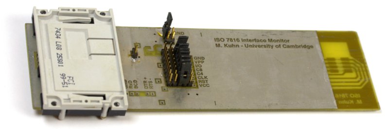
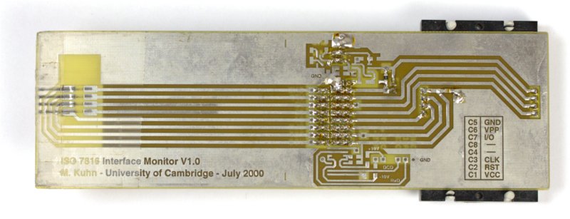
Some of you may already know that during my PhD I had a side interest in demonstrating vulnerabilities of the EMV Chip and PIN payment system, together with colleagues from the Security Group of the Computer Lab. The discoveries and demonstrations we've made helped a great deal of people who were left to their own devices against banks who wouldn't refund them the money that was stolen from them, claiming that Chip and PIN is more secure than it really is.
Anyhow, during our investigations an analysis tool created by my former PhD supervisor Markus Kuhn, was a great help. Markus designed and manufactured a card, pictured below, to both emulate a smartcard and sniff data going to and from a card and a reader.
Markus' board is thirteen years old, and my colleague Steven Murdoch asked me to design a new card that had soldermask and gold plated contacts. I put my own touch to the layout, and this is the result: In the spare space, I've included in silkscreen useful information such as common commands and their meaning. Hopefully, this will save time to users by not requiring them to wade through the thousands of pages of the EMV spec with every frame.Now I'm gathering quotes for a 0.8 mm board with selective gold plating. Anyone has recommendation for a PCB house that can do that cheaply?[UPDATE: 'itemv' was manufactured!]
↧
Just a quick note to say that I've updated boldport's homepage with new content and a new look. I hope that the focus on "beautifully functional circuits" would attract the right audience -- those looking for making visually pleasing and functional boards. Please let me know what you think.
↧
'shimmy' is a Raspberry Pi "hackable" daughter card and is the second board manufactured with PCBmodE. The primary purpose for 'shimmy' was to test dual-sided boards, and the generated Excellon drill file. Six shimmys are now back from OSH Park; below is the analysis.![]() |
| 'shimmy' top |
![]() |
| 'shimmy' bottom |
![]() |
| Small hole |
![]() |
| Large mounting hole |
The 155 drills are all aligned, so I'm confident that the Excellon data is correct. I should have made the copper rings around the pads a bit larger, particularly for U3, though. The large mounting hole (shown on the left) was meant to be non-plated with a ring around it, and that came out as it should have. The smaller hole (shown to the right) in the left corner of the board was meant to come out non-plated as well, but came out plated. (In the figures the light green is lack of soldermask, and dark green is copper.) I assumed -- wrongly -- that since there was no copper surrounding the small hole, it wouldn't be plated, and the small bit of copper within the drill diameter would be drilled out. In the future, I'll have to either draw a ring as with the mounting hole, or be more explicit about non-plated holes (there was a single drill file, so I wasn't as explicit as some manufactures require, btw).
QR code:The QR code is made of an exposed (that is, lack of soldermask) copper plane on the bottom layer. ![]() |
| QR code |
When I printed the QR code with 1:1 scale it worked without a problem, though when I got the board, the Android app on my phone wouldn't read it no matter what I tried. Over breakfast I happened to see another QR code on a piece of paper and realised the problem -- the QR code on 'shimmy' is colour inverted! <facepalm>. The bits that appeared dark on paper, appear light (silver/gold) on the board over the dark (purple) soldermask. It turns out that most QR code apps do not support inverted codes, though I found an app -- NeoReader -- that does, and it reads the code without a problem. Next time I should take this inversion into account and simply invert the code and perhaps add a border around it.
Silkscreen:The silkscreen did not come out as nicely as with 'pieceof', which was manufactured with (the more expensive) Eurocircuits. That said, everything is legible so that's not a problem. (Next time I'd make the drawing near D8 a bit larger, though).Unfortunately, four of the six boards have misaligned silkscreen on the bottom side. Since this misalignment appears only on a subset of the boards, I suspect that it was caused by a manufacturing problem, and not due to PCBmodE's Gerbers -- I'll need to confirm this with OSH Park, and make sure that nothing was missing from the Gerbers / design that could have helped prevent this.
![]() |
| Silkscreen is a bit off |
![]() |
| What the silkscreen should have looked like |
Soldermask:'shimmy' is meant to be 'hackable', by which I mean that cutting and patching traces is expected. For this, I exposed some of the traces so that they could be easily cut or scraped off. For example, all the resistors in series with the I/Os are shorted so that the board works without needing to solder anything on the pads (like a 0 Ohm resistor). Another example is J2, which carries the 3.3 V rail from the RPi through the GPIO header to the rest of the card. The idea is that if one decides to use the optional LDO on 'shimmy', the short can be cut, and a patch from the LDO header can be connected to the bottom pin of J2 to supply the card with that rail instead. (The amount of current that can be sourced from the RPi's 3.3 V rail is very limited, so the additional LDO could come in handy.)
![]()
Overall, a good run. I promised four people over on Twitter a free 'shimmy' and I hope they'll make good use of it -- I plan to dispatch them later on this week. I'd like to create more of this card with some modifications, so if you're interested in buying one please let me know.
↧
Bob Pease was an analogue design guru who untimely died in 2011 in a car accident. I didn't personally know Bob, or much of Bob until recently for that matter, but I get the impression that on top of being an analogue design authority, he was an interesting character. Bob produced one of my favourite quotes: "My favorite programming language is solder", which I loved even before I knew to attribute it to him.I created a tribute board for Bob that includes the above quote, and a light intensity to frequency circuit that uses one of the integrated circuits he designed, the LM331. On the front there's the quote and pads for both surface-mount and through-hole components. On the back there's the circuit diagram as a silkscreen overlay (the circuit is taken from Figure 20 of the LM331 datasheet). The corner holes can be used for power input or mounting holes. Maybe this board would be a fun way to introduce kids to soldering!
Here's how the board is rendered by webGerber (there's an error with opening the drill file, so the drills are missing):![]() |
| Top |
![]() |
| Bottom |
Here's what it looks like in Inkscape:
![]() |
| Top and bottom |
![]() |
| Top |
![]() |
| Bottom |
Finally, the look from gerbv:
I wonder what would be Bob's reaction to this board ;) If you'd like one of these boards, let me know so I can make one for you!
(UPDATE: see a more recent draft of the board here)
↧
↧
When I talk to engineers about PCBmodE, the topic of 'component libraries' often come up. "Converting the EAGLE libraries to PCBmodE could be a huge boost", etc. It does make sense at first, but then it gets depressing when you think about what it means: we've gotten so accustomed to shitty EDA software, that the notion of recreating simple things such as footprints from scratch is unthinkable. No. Good software would let you create basic components with your own preferences very easily, from fresh, freeing you from dependency on libraries that never quite have what you want. Let's admit this: in practice, component libraries aren't that useful -- their style doesn't match yours, they're made for the 'wrong' software/version, or you need to make some tweaks. More often than not, you end up making a new instance anyway! True or false?
I'm a big fan of reuse, but this isn't about reuse. Component instances should be like freshly minced garlic -- you'd never need to use that stale crap from a tube because it's so damn easy to make fresh. Yes, this is about usability, and the sorry state of EDA tools again -- we've been conditioned to think that things are hard because every time you use these tools the 80s calls and tells you that deleting components from a library requires watching a ten minute video. We've got such wonderful software tools for software developers, and much better understanding of user experience than we had 20 years ago, and it's time we started using them for engineers.
↧
A couple of weeks ago I've introduced the 'pease' board, a tribute to Bob Pease. I've tested that the circuit works on a breadboard:
I also made a few changes to the board, mainly stylistic, anded a handy ruler! I hope to be able to teach soldering and basic circuit design with this board. If you'd like to buy some unites from the first build, please let me know as soon as possible.![]() |
| Render from webGerber |
![]() |
| Render from webGerber |
The renderings from webGerber didn't accept my drill file and seem to not handle the right and left edges very well for some reason. Rest assured the drills are there! ;) Here's the PCBmodE view:
What do you think?
↧
Recently I've written about the myth of the large component library. I made two claims. Firstly that libraries rarely have what you actually want, and secondly that the inability to easily create footprints exemplify the poor state of EDA usability.
In a comment, Karsten Becker made the argument that a library footprint is more likely to be "correct" -- in quotes because "correctness" in this context is relative -- since it was looked at by more people. CircuitHub also claims this. I want to challenge the notion that this is, in fact, a good thing. By creating our own footprints we end up getting exactly what we want, how we want it -- which is, as it happens, exactly different from what everyone else wanted in the past -- and, more importantly, it is another opportunity to get more familiar with the device. It's one thing to forget a bar on the pin's labelling, but quite another designing in the wrong component! Acknowledging each pin's existence forces us to think about its function, and discover well-hidden caveats and constraints buried somewhere in the datasheet. We're also far from guaranteed that the device in the library is, in fact, "correct". Maybe only the creator looked at it? Maybe this creator forgot to correct a mistake after their board needed a re-spin? Maybe a lot of people looked at it and didn't notice a problem? Maybe what was good enough for everyone else (location precision, for example) isn't good enough for me? Maybe the mistake was never relevant to anyone, so it wasn't noticed? Maybe I'm going to use a different revision of the part? Maybe the footprint was created from an old version of the datasheet? Too many doubts considering what manufacturing mistakes cost me. I'd verify the hell out of any footprint no matter who looked at it -- even if it was me six months ago -- so the amount of time a component from a library could potentially save me is quite small.
Finally, accountability is kind of a hobby of mine, and I like owning my own mistakes. I would take ownership of any mistake on a board I design no matter the source, so I'd prefer the mistakes were mine, and not imported ones.So this leaves us with the original argument -- creating fresh footprints should be easy; libraries don't cut it, at least not for me.
↧