Quantcast
Channel: boldport
Viewing all 50 articles
Browse latest View live

A look at 'itemv'

$
0
0
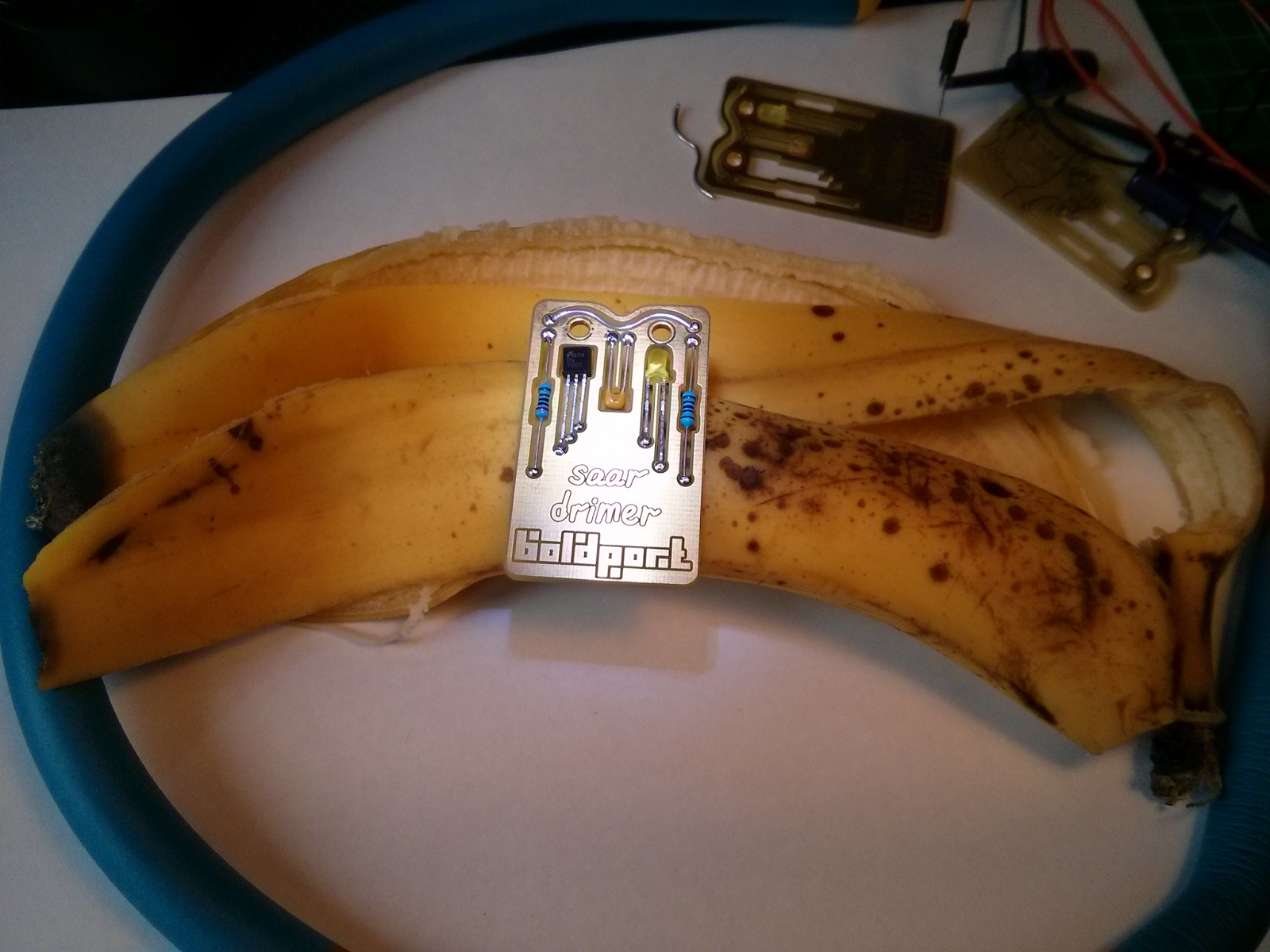
The 'itemv' (ISO 7816EMV smartcard analysis) board came back last week, and it works great! I wanted to point out a few things that are noteworthy about this board.


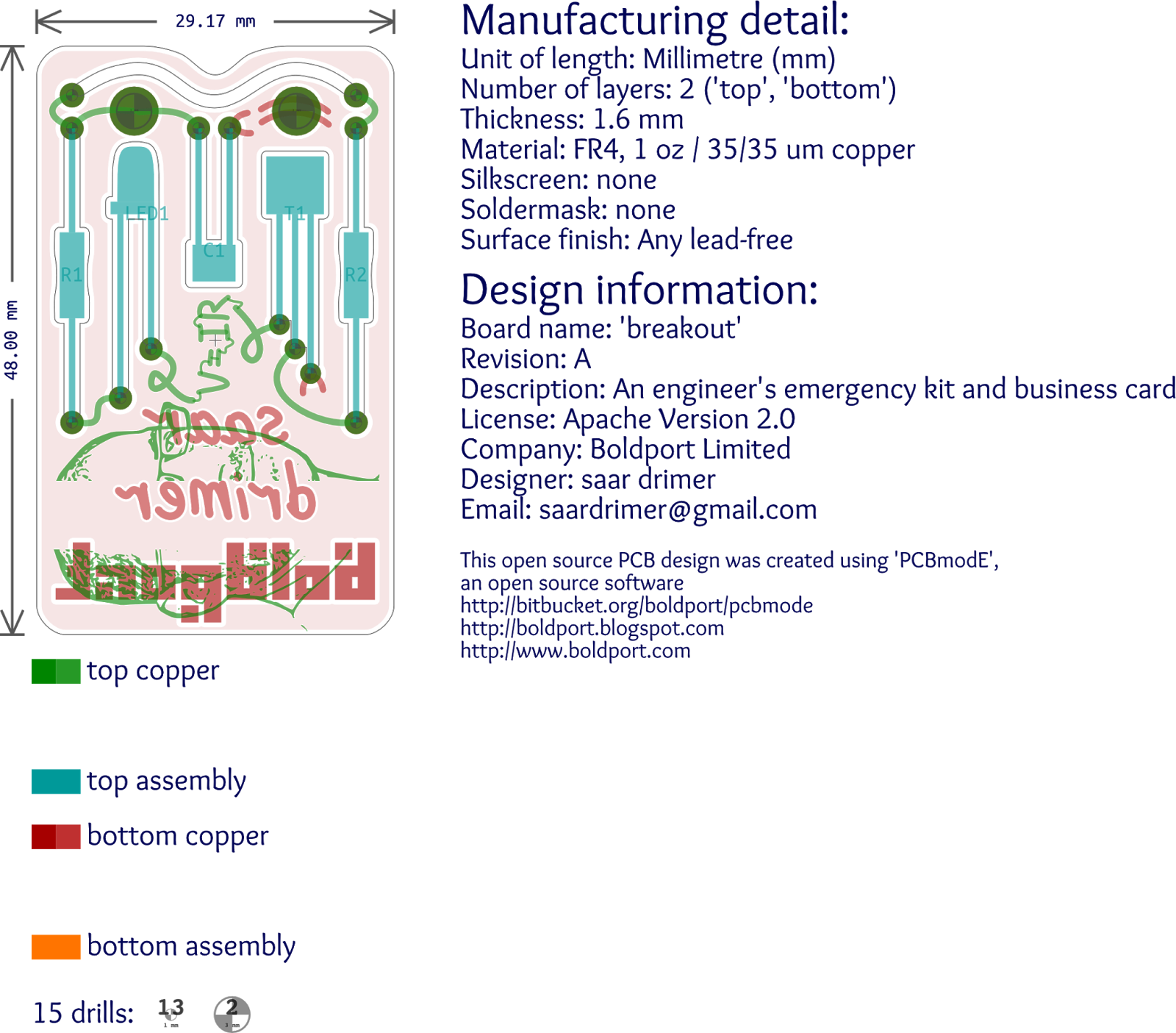
The ample "spare" space on this board is used to list EMV commands and what they mean, so the PCB itself doubles as a reference card. I imagine someone snooping on a transaction, and decoding the messages on the screen using what's written on the PCB instead of going to the thousands of EMV spec books -- pretty cool, no? I'm really impressed with Eurocircuits' silkscreen process -- it allows very fine details and this small of a font size that's still very crisp and readable. On the bottom side there's also a silkscreen block that can be used as a scratchpad.


The traces really give out an organic feel when light is shown through the board. I really like this extra visual dimension, and try to incorporate that into all the boards that I make. In a stretch I could justify this layout by claiming that the ground plane between the traces shields them better, but it would have worked just fine without it.


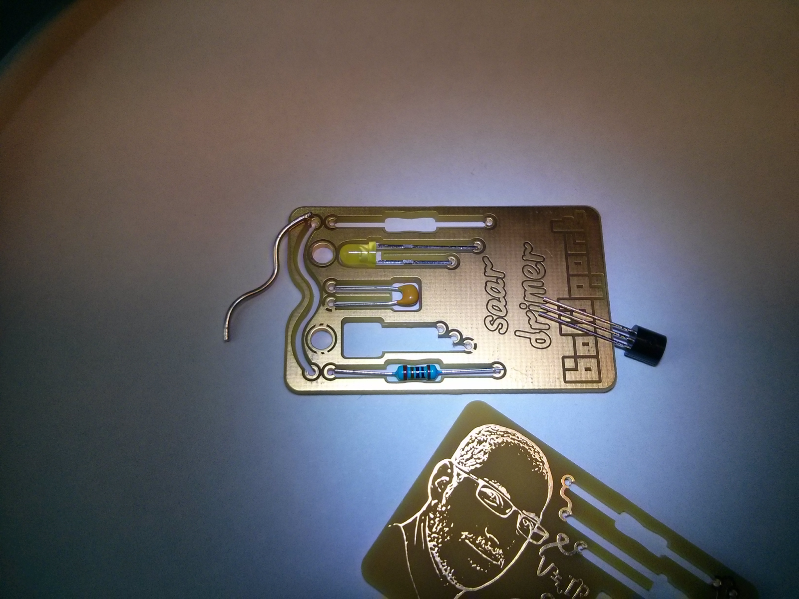
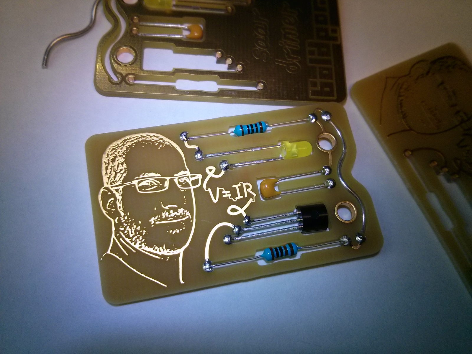
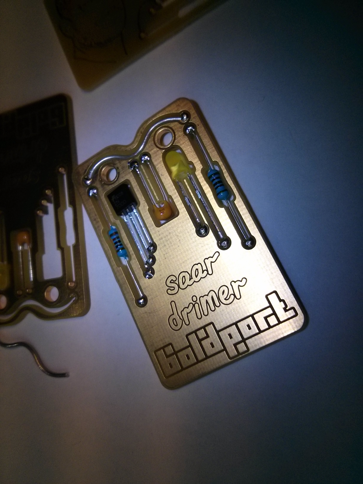
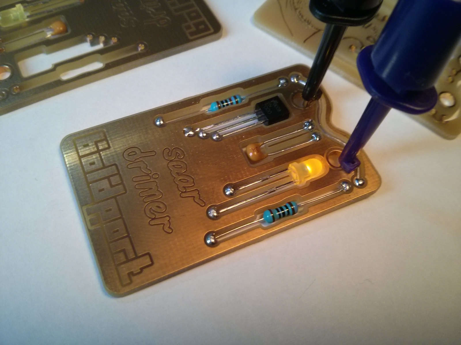
This board was also designed to allow power analysis of EMV cards. The setup of the pins allows having either a throughole or SMT small value resistor on the ground and/or power trace. There are also turrets for the scope probes, and a general purpose header for a jumper, or a simple wire hook. The two dual header pins configuration allows putting anything you want between the actual card and the board's "card", or simply creating a short using a jumper.

Finally, one of the annoying features of the old "smartcard interface monitor" I've used in the past was that it was hard to grip when you insert and eject the card from the reader. I solved this by adding indentations on the sides for fingers -- really simple with PCBmodE.


The end of myths -- solving one of our industry's nastiest of problems

$
0
0
In a series of past blog posts (first, second) I've described some of the myths surrounding component libraries. They were, in fact, merely symptoms of a chronic ailment of our industry -- I was using them as examples in order to ease my way towards the real problem.

Have you ever asked yourself why is it that 'design rule checks' (DRC) in your EDA tool do not point out apparently simple things such as signal polarity mismatches, wrong input voltages, wrong signal--pin connections, or wrong footprint dimensions? Or perhaps more "sophisticated" things like wrong/poor termination, impedance mismatches, or insufficient decoupling? Have you asked why is it that most DRCs are generally satisfied with simply automating the checking of distances between traces, pads, and pours when additionally pointing out electrical problems could save a lot of money to companies?

They cannot. I'm sure that many EDA companies thought of achieving the above, though it became very clear very soon that the data that must be available to achieve this "miracle" isn't there in a usable form. I'm talking about component meta data: dimensions, properties, functionality, and basically everything that's in tables and graphs in datasheets. For historical reasons, lack of standards, and probably a healthy portion of old-school lock-in fantasies, companies do not provide such data in a way that can be automatically processed. The best one can do today is parse PDFs or rely on "crowd wisdom", both of which don't really work for this problem.

It's a testament to the entrenched backwardness of our industry that despite knowing that a solution to this problem could very well unlock a world of innovative DRCs and tools -- and a lot of savings -- we and "they" still could not convince manufacturers to provide digestible component metadata, even if it was in something as simple as a CSV file*.

What can be done? Firstly, demand better tools -- don't fall into the 'digital Stockholm syndrome' trap of praising a bad tool just because you've spent years mastering it through an abusive relationship. Secondly, demand better data -- support manufacturers that aren't lazy with providing data, if and when those exist. Finally, be aware of the problem and support whoever is trying to do something about it.

* This isn't necessarily unique to the EDA business. I know of at least one thriving research field that could be completely eliminated if scientists bothered to provide metadata about their findings in a consistent way together with their publication.

New board: 'redditoken'

$
0
0
I've been a lurker on Reddit since pretty much the beginning, and can say that aside from periods of rage-quit that lasted a few weeks at a time, I've been visiting the site pretty much every day. Reddit has a culture that many redditors cultivate; in the early days it was an obsession with Paul Graham, but now it's more about bacon, narwhals, and images of kittens and puppies. This is not a digg at Reddit, simply noting what tends to be prominent on the front page these days ;)

Anyway, I thought of creating a Reddit-themed token. Here it is...

Both sides


top layer
bottom layer

Since the "The alien's eyes are always #ff4500" (orange), if you connect a 5V and ground to the top and bottom terminals/mounting holes, respectively, two bright orange LEDs will light up.

Here's the OSH Park view:

top layer -- a rendering of the board by OSH Park

bottom layer -- a rendering of the board by OSH Park

Finally, a view from webGerber, though I couldn't make the drills appear (again!) I tried real hard.

top layer -- rendered by webGerber

bottom layer -- rendered by webGerber


I already noticed something I should fix; see it too?

I'm not sure that these images reflect well what I imagine it will look like in its physical form. We'll see. Please let me know what you think! I'll probably send this off to OSH Park in the next couple of days.


'pease' are back!

$
0
0
The 'pease' board are back from Eurocircuits, and look great! I hope that Bob, who died two years ago, would have liked them, and their purpose -- celebrating his work, and teaching people how to solder.


Updated website

$
0
0
Just a quick not to point out that I've just updated Boldport's homepage: http://www.boldport.com. There are new images, slightly changed layout and a brand new page for the 'pease' board. It's amazing that there has been so much progress in just two months since the new site went up! Please let me know what works and what doesn't on the website, and have a great week ahead!

Showing off the 'redditoken'

$
0
0
A month ago I've written about the 'redditoken', a Reddit themed circuit board. The tokens are back from OSH Park, and here's a short video about them


What do you think?

New board: 'wuthering'

$
0
0
The omnipresent Andrew Back has asked me to design a small board / badge for the upcoming Wuthering Bytes Workshop in Hebden Bridge. We decided on a simple circuit -- something based on littlewire (thanks!) -- and Andrew gave me creative freedom. Below is the result. It's released under the Solderpad license. The source is here, and the Gerber package is here.

Please help us by having a look over the design files, and let us know if you spot any problems!

Lots of nice pictures below...


Webgerber render (as usual, no drills)
Eurocircuits render top
Eurocircuits render bottom
OSHPark render top
OSHPark render bottom


As seen in Inkscape


A new teaching board for The Centre of Computing History in Cambridge

$
0
0
The Centre for Computing History has moved to Cambridge, and has been officially open for a couple of months. Jason Fitzpatrick -- the man who has made all this happen -- and his team of volunteers have transformed a barren warehouse into a wonderfully hands-on display of computing history. It's just the beginning, and we should all look forward to having Jason's vision materialise.

Jason saw the 'pease' board and immediately realised its potential as a tool for teach people basic electronics and soldering skills. The 'pease' is accessible, non-threatening PCB with interactive elements, which we hope would attract young people to the art of electronics.

We've worked with Jason on simplifying the board. The new board is smaller (56 x 19 mm), has fewer components, and power is supplied through a "hanging" micro USB connector. There's a large hole in the centre, so that the board could be hung on a nail in the wall or around one's neck ;)

We plan to make these available as nicely packaged kits that will be used in soldering/electronics classes at the Centre. Attendees will get to keep what they have built! 

The design files are in the usual place, and here are the usual pictures.


Eurocircuits Visualiser rendering (top)
Eurocircuits Visualiser rendering (bottom)


gerbv view (top)


Engineers, assemble!

$
0
0
The EDA industry is hostile to innovation. I thought that that was a pretty strong statement until I uttered it in a talk and an industry veteran remarked that that was actually an understatement!

Innovation in our field faces two fronts -- adoption by engineers and an industry ruled by old-school "Big EDA" that are stuck in the 90s in pretty much all aspects: usability, methodologies, distribution, style, pricing. Innovators are prevented from publicly benchmarking the performance of their products against Big EDA products through over-reaching EULAs and lawyering up. The entrenched lock-in and proprietary mentality is strong enough in our industry to the extent that it makes it very hard for engineers to even try something new. Turf wars and design-by-committee symptoms prevent an open, free, and modern data exchange that could drive the innovation the industry is craving for in order to deal with ever larger designs and teams. It's quite a strange state of affairs.

(Even if you're not familiar with the industry you'll appreciate this example: many EDA websites will still, or have until recently, require you to register and log-in in order to view some/all of their documentation! How 90s is that!?)

The only way out of this predicament is to use the power we have. Engineers, try new software and support it, if only by giving feedback to its creators. Reward innovation. I'm writing this post with some frustration after receiving a few emails from people who said that they were disappointed to find that  'boldport flow' -- a browsed-based automated FPGA build generator -- was gone! I really would have liked to know it was useful to them back when I was contemplating, and then, shutting it down.

Thankfully, things are different with PCBmodE. I'm getting unsolicited emails from people on a regular basis, which is a huge boost of confidence that "there's something here". Back in the 'boldport flow' days I had to beg for feedback, which was one of many signs that something was wrong.


The 'lifegame'

$
0
0
My friend Mike is getting married on Saturday (tomorrow). Both him and his soon-to-be-wife enjoy video games -- as do I! -- and I thought that a game-themed gift would be nice. Since I'm all into this artsy PCB thing, I combined the two into the 'lifegame' board.


The basic idea was to create a piece that came on a single PCB panel, where parts are snapped off and soldered in place in order to create a frame such that the final piece can be mounted onto a wall. (Is this the first wall-mountable electronics?) No glue and no external mechanical components except for two screws for the wall mount. I wanted it to be big and for it to have a presence!


I started out with a quote I had in my mind for a long time, Life is the game, and searched for an appropriate font. I ended up using a font by Brian Kent called 8-bit Limit. Then I researched gaming icons. At first I intended to draw them myself, but then I found this wonderful library by Lorc, and used a small subset of 42 icons along the side panels of the frame. I've added the menacing boardame-like silkscreen, and I had the rough visuals sorted.


I wanted an interactive piece that has some electronics Mike could play with himself -- he's also a computer scientist. I ended up with 42 WS2812B addressable RGB LEDs and an ATtiny85 to control them. The idea is that these LEDs would light up the wall the piece is mounted on, diffuse, and then shine through the gaps of copper and soldermask. Luckily, Adafruit has a very convenient Arduino library for controlling these LEDs; it worked out of the box, and saved me a lot of time. I went for 42 because it was an obvious number, but also because I wasn't sure that fewer LEDs would be enough to light the thing up properly. In case I decided to go with fewer LEDs, I designed the LED's footprint in such a way that I can simply put a solder blob in the right place and the chain won't be broken. Well, it turns out that 42 is plenty, but I'm keeping it in case Mike wants to use 'lifegame' for one of his disco parties.


The panel -- front
The panel -- back

To add to the gaming theme, there's a large functional arcade button that's hooked up to the ATtiny85, so it could be used for anything. Since the frame is only 18 mm deep, I had to cut the button to fit, which was more work than I anticipated. Originally, I researched how to hide the power input and power switch, since I wanted to keep the design clean. After some thought, though, I decided to completely go over-the-top with a large missile launch switch (that just barely fit) with a flip cover, and an industrial strength screw-in power input. All exposed and celebrated!


There's a wall mounting mechanism where square ribs are soldered onto a strip that is mounted onto a wall with two screws. This creates enough protrusion for the frame to hang on. For suspenders, the ribs have holes through which wires go that are attached to the board on the other end. This way, if the frame ever falls off the mount, it won't reach the floor. Finally, there's a small plaque for mounting under the piece.


It's the largest board I've created with PCBmodE, and the first of my boards to be manufactured by Express Circuits here in the UK. Express did a wonderful job, working with me on a custom soldermask colour, and putting on a thick gold coating for the exposed copper to create this striking contrast. Since this was a wedding present they offered me a discount(!) and made sure the board came back to me well ahead of schedule, so that there was enough time for a re-do if necessary. Good stuff! I've worked on this board for a couple of months, only seeing it in my imagination. When it came back it was just like I imagined/wanted.


As with most of Boldport's board, 'lifegame' is open source, and it's available in the usual place in the repo. (I've corrected a few issues, so the version online is rev B.) If you make one for yourself, please send me pictures! If you want me to make you one, contact me for details; if there's enough interest I'll consider making another batch.


A view of the board from within Inkscape
So, what do you think?

Just applied for YCombinator

$
0
0
I suppose that it isn't that ordinary to publicise this sort of thing, but I just hit the button for the Winter 2014 YCombinator application. I'm not that hopeful, though -- I think that my application is a bit weird in comparison to what I think they expect. Particularly, I didn't have some of the answers, and I'm a single founder, which is generally thought of as a "bad thing". I actually enjoyed the application process! The questions are casual and the video isn't a competition in lighting, and it took very little time to complete.

I applied because I need help making Boldport more than just a consulting business. I'm not even sure YC is (also) about this kind of help, to be honest. But why not apply? They might see things in what I do that I cannot or do not -- they are much more exposed to some industries than I am. I guess that the worst that could happen is mild embarrassment and another entry in the rejection compartment. I can handle that.

The other reason I'm applying is because YCombinator is the one of the top incubators in the world. Back when I was applying for a PhD, I decided that if I get into the top five schools, I'll go. I only applied to MIT and Cambridge. It was good timing, and I wanted to experience grad school. I feel the same now about this application. Kind of a neat parallel.

Anyway, this doesn't change much, but I still wanted to share. 

Now back to bonkers.

The origins of PCBmodE

$
0
0
I've been obsessively doodling all my life. I've got notebooks and pieces of paper full of abstract drawings of meaningless stuff, from my teenage years until today. Any time there's a piece of paper and a pen or pencil about, I start doodling. Iusedtopublishsomeofmymorerecentandelaboratedrawingsonmypersonalblog.

As a person of very few hobbies, I decided to pick up painting on canvas. I'm not very talented in drawing real things like fruits, landscapes and humans, so I experimented with abstract colourful paintings and even ones where I tried to add a physical third dimension. I used themes that are very common with my usual doodles.


In a process that happened naturally, I gradually gravitated towards painting circuits and logic, and I experimented with several techniques and concepts.


And this is probably the most complete work that's circuit related.


So how all of this related to PCBmodE? While I was painting these abstract circuits I started asking myself why am I not making circuits -- another thing I love doing -- that are art. I was painting circuits, but I was thinking of designing circuit art! My initial thought in this direction was to create a large wall-mounted piece piece that had electronics embedded in it that enhanced the visual experience.

Also, for years I've been having thoughts on how to successfully innovate in the innovation-hostile EDA industry, following a decade-long frustration with poor usability of EDA tools (and one failure to get a company going in this area). I generally and passionately despise the limitations EDA tools impose on creativity, productivity, and imagination.

Suddenly those two seemingly unrelated threads came together at a time when I had to be flexible with my schedule, and when I was finishing a job. I then started writing a PCB design tool of my own, PCBmodE, as no other tool could give me the creative freedom that I needed. Roughly a year later I created the 'lifegame', which is the realisation of the initial vision I had for the software.


An update

$
0
0
Lots has been happening on the Boldport front. There's 'cuttlefish', an educational board made for Embecosm; 'deadwood', a tribute to the cordwood PCB assembly from the 1960s, which will be sold by oomlaut as a kit!; 'logical', a board for PSHDL / Kasten Becker, which I'm late to deliver on; 'iron' and 'case', exciting secretive projects for an unnamed client; 'breakout', an engineer's emergency kit doubling as a business card; 'pease-cfch', a simplified 'pease' made for The Centre for Computing History that will be sold as kits; and, 'star', a simple experimental circuit for Star Simpson. These are the ongoing projects, and there are several exciting new ones in the concept stage.

The 'deadwood' board, a tribute to the cordwood construction. This board can be plugged into an Arduino header to control all eight LEDs individually.


If you've been following @boldport, you'd know that the application for YCombinator Winter 2014 funding was rejected. I was expecting that, but it was well worth a try. They do not provide feedback, so I can't tell what exactly they didn't like. If Boldport's story improves, and the situation's right maybe I'll apply for the next round. Against their recommendation, I neglected to save a local copy of my application; otherwise I would have published it here. The application video contains some things I'm not yet ready to talk about publicly.

I'm excited about CERN's investment in KiCad -- an inten developer for a year; I have a feeling that this is a significant step towards a robust open source CAD/EDA tools that can rival proprietary tools and their backwards ways. I'm particularly interested in how this will work out since I'm trying to pull something that hasn't really been successful before -- an open source engineering tool developed and maintained by a (profitable) commercial company. I find it hard to convince business types that this might actually work -- to be honest, I'm still convincing myself, and it might not work! -- because everything pulls towards the established closed-source model.

While we're on the topic of business, I'll mention PCBmodE's "donation" page. It's a way for you to support PCBmodE's development by buying something at an outrageously marked-up price. So if you like what we're trying to do, and find PCBmodE useful or interesting, please consider buying something.


An engineer's emergency kit business card

$
0
0
Circuit board business cards have been done. But since circuit boards are, literally, my business, I felt that I needed one too. Of course it also had to be special. Research and experimentation took a long time with this one and the design even sat dormant, ready, for a while before I sent it out to fab.
Without components
The concept was to have throughole components embedded within the PCB and soldered lying down. The components -- two resistors, LED, NPN MOSFET, and a capacitor -- form a complete circuit so that when voltage is applied, the LED turns on.

Sizing up the components. Notice the wiggly piece of solder that fits into one of the slots.
It's meant to be an engineer's emergency kit. When all hope is lost, the MacGuyver engineer could snap out one of the components and save the day. Recall the countless times you desperately needed a 1 KOhm resistor to fix an amplifier at a party, only to see the girl you were trying to impress slip away with an OCaml programmer? Never again with this little kit. You even have 2 cm of solder in there to make sure the connection's electrically solid!
Components soldered into place (top side)

Consider the times when you were too drunk to recall Ohm's Law, yet was called in to fix a spaceship's control system. V=IR is written on the board to rescue you into awesomeness in spite of your inebriated state.
Components soldered into place (bottom side)


For those extreme situations when you need a Winston Wolfe my details are there so you know who to contact when the going gets tough. Finally, as motivation, my disapproving mug is there to stare at you as you're going about your engineering super hero day.

It's a functional circuit! The LED lights up when you apply power.

The board was manufactured by PCB-POOL, without soldermask or silkscreen and using their default ENIG finish. This was the first PCBmodE board I've made with this fab, and they've done a great job. I particularly like that they send pictures of the board during the manufacturing process.


Banana for scale for us Reddit types
Now I only need to figure out how to manufacture this design cheaply enough so I can actually give those kits away ;)

A view from Inkscape/PCBmodE. The assembly layer was used to size the cutouts. (That break in my face is an artefact from Inkscape's bitmap export.)

(Oh, this is an open source design! The source files are at the usual place in the PCBmodE repository.)


In defence of the "sloppy" engineer

$
0
0
When things go wrong it's tempting to blame the "sloppy, incompetent" engineer. Security breach? Bad board? Cumbersome UI? Ah, it's that stupid engineer again! Not the overbearing boss, lack of resources, inappropriate tools, non-existent training and mentorship, shortage of staff, impossible schedule, or ignorant management. It's that pesky sloppy engineer that's responsible for that voting machine fiasco.

That kind of language really presses my buttons. The latest press was on the thread about my engineer's emergency business card over on Hacker News where "In summary, even the best tools won't help a sloppy designer" was used to excuse unfit-for-purpose EDA tools by blaming the engineer. This isn't right and is not leading us to a better situation. (The specific comment and my response are here.)

The engineering tools we use are crap -- if that sounds a bit crass, it's because 'crap' captures the essence of the experience better than any other word I can think of. They look like a Windows 95 space shuttle cockpit, overwhelming, do not present information in an effective way, often do not check for what really matters, and stand in the way of good design practices that would help less experienced engineers. If you are forced to use these tools -- and you are because there's no other choice -- and are inexperienced, are you necessarily "sloppy"?

Instead of saying "read the thousands of warning and info messages from an FPGA design build" ask "why is the tool not smart enough to show me what's really important?". Instead of saying "make sure that the 5 V net is named the same across the entire design by clicking every segment" ask "why isn't the tool smart enough to figure out that those nets are connected, or display a small warning on the schematics instead of hiding it behind a click-wall and hundreds of other entries?". Instead of saying "print out the design 1:1 and lay the components on the paper to make sure the dimensions are OK" ask "why can't the software compare those dimensions against the datasheet?" (More about this one here).

There's a "get on with it" mentality in engineering culture, which is great -- it makes us crafty and innovative. But there's also a certain kind of unexplained acceptance of inadequate tools that might stem from that need for tinkering. "My EDA tool is morbidly broken, so I'm going to happily fix it with a script" can get our juices flowing. But this doesn’t mean that we do not deserve better, and it certainly doesn't mean that (inexperienced) engineers using current tools are "sloppy". Let's not go there please.


I'm an engineer!

$
0
0
Teenagers used to have posters of Einstein on their walls. Decades pass and now they have Miley Cyrus adorning their rooms. What's next, a cat playing the piano? Scientists and engineers' contribution to society is far greater than these manufactured celebrities, yet we're not celebrated by twerking a wrecking ball in front of a huge raging crowd. (Not that we'd want to, but you get the point.)

The new 'superhero' is a circuit board that eloquently projects what we engineers often feel inside,

The board is 10x10 cm with ENIG finish and green soldermask
and is the first step in regaining the recognition that we deserve! Here are a few scenarios where this board may come in handy in day-to-day life.

The bottom side isn't covered with soldermask, so light shines through and the board's appearance changes


Say Jimmy comes over to your cubicle to thank you for finding that signal integrity bug the company's flagship product has been having. Don't say anything; don't turn around. Simply point to the 'superhero' plaque sitting there on the shelf amongst your soldering kit. BAM!


Say you're called to a crime scene in order to determine whether the perp used Emacs or VIM, effectively deciding the case. Forget that tiny badge they gave you at that IT Academy and simply flash the 'superhero' that's hanging around your neck. They'll make way and respect your authoritay.


Finally, for those small 2am moments working on a pet project -- look up from that awesome soldering job and shout FUCK YEAH!


Want one? Express your interest in the comments or email me so I know how many to make next time. Want one NOW? I'm running an open auction over on Twitter for one of the two boards I've made in the first batch. All funds will go towards PCBmodE development, and you'd get a dedicated, signed version of the board! You can bid by following @boldport and placing a bid using the hashtag #EngineerSuperhero. (There are also other ways to help support PCBmodE.)

UPDATE: The bid is currently at £75 from oomlaut! Join the bidding and be part of history!
Close-up of the cross between the copper "etch", exposed copper, and soldermask exposure of the copper pour to create full symbols


Finally, a huge thanks to Beta Layout for making two instances of this board, for FREE! They've had issues with processing my Gerber files and instead of giving up, fought their tools and wanted to make sure I see the physical results. They didn't want to charge me for them. There are still some issues to work out, but unless I tell you exactly where to look, you wouldn't notice them. Really impressive customer service!

PCB-POOL sends out pictures of the board as it is being manufactured; a really cool feature


This one came out quite nice

So you want to start an EDA business?

$
0
0
It's New Year's day. We look ahead. Some of you may be thinking today of starting an EDA business. I've been an EDA user all of my professional life and have tried and failed in starting an EDA "startup", and am now running another business in this space*.  Over this time I've had many realisations, ideas, conversations, highs and lows, all surrounding "EDA business". Since I find myself repeating some of what I've learned, I wanted to share my thoughts and opinions here.

Three points to start off with:

  1. EDA tools generally suck in most ways possible. Pretty much everyone agrees on this. There is a huge need for innovation on several fronts: optimisation, usability, team-based design, to name just a few. Lack of innovation on any of these will eventually grind the industry to a halt.
  2. The EDA business is dominated by a handful of well established, huge, resourceful corporations, with users that are generally conservative and bound by old-school ways and corporate constraints.
  3. As an industry we're very poor at exchanging information in an effective way.

All of what I'm about to say is a result of the points above.

Engineers are conservative

It's a gross generalisation, but when it comes to trying something new, we engineers are not as enthusiastic as our software dev counterparts. We tend to stick with how we're used to doing things, particularly as we progress with our career. It's quite sensible to do that because mistakes in hardware tend to be very expensive, and you're expected to get things right on the first go. This doesn't help innovation, though. (In a somewhat perverse way our affinity to tinkering may explain why we tolerate broken tools -- we like fixing them with clever elaborate scripts!)

Most engineers in big companies are possibly not even allowed to try anything new. That may be a sensible policy from a corporate point of view, but it too does not help with innovation.

Finally, it's rare that the engineer has any say in the tool choices. Those important decisions are the domain of "purchasing"! Doesn't help.

The lifestyle chasm

Over the years I've spoken to many EDA small business / startup owners. The picture that emerged is that unless you have a protectable innovation that is tackling a burning problem, get huge amounts of funding to develop it, and sell to one of a handful of companies, you will be sliding towards the "lifestyle chasm" and never climb out of it. Some of the people I spoke with were at it for more than five years, some got millions in funding and still shut down after that time. Some regretted sticking with it for that long. They had what I considered to be a great product.

10X is 1,000X hard

Say that you developed a product that everyone universally agrees that is 10X better in one important area compared to the nearest competition. Problem is that the EDA business, traditionally, is based on lock-in and reliance on high switching costs to stifle competition. That mandates a huge financial and educational commitment and reliance to and on a particular vendor, and their way of thinking and doing things. So now, despite having a recognised superior product (in one area), you have to overcome their investment in the "other" product. But, more crucially, the "other" product needs to only slightly improve in order to kill your 10X and prospects.

Prehistoric

While it's getting progressively better, we are still stuck somewhere in the 1980s in how we communicate data. Revision control is an emerging technology, designs are sent by email, Gerber and Excellon formats are still ubiquitous, exchange formats are proprietary and designed "by committee", and every component has a different format of a datasheet with no machine readable information. It's very difficult to innovate where the basics aren't even there.

"Big EDA" can be ruthless

The large players in this industry guard their entrenched positions well. They even discourage performance benchmarking in their EULAs. It's actually very hard to publicly prove that your product is better! As a small business, you can't compete with the lawyer power of those mythical beasts. Here it’s worth mentioning that purchasing cycles in EDA are loooooooong. If you're to survive, you will need a large reserve to cope with the one to two year it typically takes for a company to actually buy your product.

So you want to start an EDA business?

"Will this guy stop whining; it's hard to succeed in any industry" some of you are thinking. That's true. I'm not writing this to stop anyone from trying, though hearing about some of the more common pitfalls from an industry-specific view can help. If you're thinking of starting a business in the EDA space, consider the following:

  1. There's a lot of room for innovation. The temptation is huge. But be prepared for the best case for your idea to become a lifestyle business. If what you're doing doesn't seem like something you'd be happy doing for a "salary", then it might be worth re-thinking the concept.
  2. Don't plan on converting all engineers. Some engineers will never try something new. Some engineers will not even think that there is a problem with their broken tools since the tool has abused them for so long they are blind due to the Digital Stockholm Syndrome. Identify early who will and is able to use your tools.
  3. Unless you have a protectable and significant innovation, don't plan to be bought out by Big EDA. Try charting a different path that will free you from the constraints that EDA is infamous for.
  4. Understand engineering culture. Understand the EDA business culture. Do not require those to change significantly as a requirement for your company's success. If anything, bypass them!

If you're an hardware developer craving for better tools, please support new projects by trying them out, providing feedback, or simply saying a good word. It means a lot.

* My first product was a web-based automated FPGA build management tool called 'boldport flow'. Good concept; poor execution. I learned a lot about the EDA business in the process. After a year of doing that I didn't enjoy it enough to continue doing it as the inevitable lifestyle business, so I pulled the plug and moved on.

I now run Boldport and created an open source PCB design tool called PCBmodE. While Boldport can be considered an "EDA business" by some, I certainly do not. I try my best to not live up to their reputation in some areas. If Boldport succeeds, we'll have to find a new acronym for that kind of business. I love what I do now, and if the worst that can happen is that it becomes a lifestyle business, I'm fine with that even though I'm aiming much higher.

oomlaut wins 'superhero' board for £105!

$
0
0
I ran an informal auction for one of two 'superhero' boards over on Twitter. After a lot of fun and puns, oomlaut had the top bid of £105! All the funds from this auction will go towards PCBmodE development. I'm sincerely thankful for oomlaut and the other wonderful folk for placing bids, and for their interest in and support of my work at Boldport. This is really encouraging. As with most of the boards I design, 'superhero' is open source. Get the source files from here, and make one for your own! (If you want to support PCBmodE dev, look here.)


But the story doesn't quite end here. When Aaron from oomlaut saw the board I've designed for 'Wuthering Bytes' he contacted me suggesting that I make another board. I started asking about oomlaut branding for it but Aaron said that he just wants me to make more nice boards so that he could sell them on his online shop, and that he'll send me a "few components" from his stock. A week later I receive a huge box full of components that could stock a small lab, even including an Arduino programmer. I protested that I should pay for it, but Aaron wouldn't have it. So, I thank oomlaut for their support. But much more importantly in my view, is the community spirit that fuel such gestures. It's going to take all of us to better places!

I won't be using an open source hardware logo on my boards any longer

$
0
0
I'm very enthusiastic about open source hardware. I've written PCBmodE, which is open source software, and unless a client does not want it to be, the boards I design with it are open source hardware by default. I offer a default 20% discount for OSHW contract work.

Without much thought I've been adding the most common open source hardware logo onto my boards. I wanted it to mean "this is open source hardware" and "I support open source hardware". Now that I have given it some thought I have come to the conclusion that it means much more than that, meaning that I may not agree or approve of. My solution is to not use it any more. This article explains why.

(I want to get something out of the way. I'm not a licensing expert, and I don't know much about the wheeling and dealing that go on behind the scenes at organisations such as OSHWA, TAPR, OHANDA, CERN, etc. who are active brands in this space. As far as I'm concerned they are all trying to do their best for the community. But life's too short for the details and politics of it. So I concede that most of what I say is based on casual reading, experience, feelings, and intuition and that it may apply to me alone.)

By branding ourselves and the things we're associated with we endorse and support that brand. We help build that brand by displaying it even when no money is exchanged. Considering the implications of this in a deeper than superficial way is hard for most things, but not so for the things we ourselves create and have control over. I'm typically very conscious of that and I'm primarily concerned about how brand association reflects on me, now and in the future -- I rarely wear branded clothes or use Apple products, for example.

Right. I slap a logo of a brand on my board, which will be there forever and project an image that is associated with that brand. I then wonder. Why am I using this logo and not another? Do I really have a good feel for the image this logo conjures when people see it? Do I fully appreciate the association this logo has with a particular agenda or license, now and in the future, intended or not? Does the use of this logo have locale-specific implications? Do I fully understand the legal implications of using this logo? Does the use of this logo conflict with the actual license I've chosen? What benefit do I get from promoting this particular brand? What will I do and feel when this logo is taken over by another brand? What will I do when the specification or restrictions change for the use and association of this logo?

There may be some satisfactory answers to these questions, but together they pose a very compelling reason to not bother. Even if there are answers today, tomorrow they may be different -- things move fast and emerging properties are frequent. We're still figuring all of this stuff out! My experience tells me that standards organisations are commonly plagued by "design by committee" issues despite good intentions, and this only gets worse when corporations start getting interested. This is otherwise considered a good thing, but may turn ugly when they become heavy handed with their cash prises.

Given all of this, I ask if the benefit of using a logo on my board is worth putting myself in a potentially unknown and uncomfortable situation? It is not. But there are other reasons why I'm not going to use an OSHW logo (of any kind) any more.

If all I wanted to say was "This is an open source hardware board; I support open source hardware", the logo does me a disservice, because its baggage-heavy nature still does not release people from the obligation to seek out the license terms for what I've created. (PCBs are a special case where there's typically no room for elaborating on the licensing terms, and they often come without documentation.) If they do that they'd know that it's open source hardware anyway; no logo needed. If they weren’t interested in the first place, this logo pretty much means nothing.

At Boldport I create open source hardware by default. I'd like the two to be associated so eventually, perhaps already today, having both logos is somewhat redundant. I think that this is quite a common scenario.

I create very visual boards, and the use of every bit of board space is considered and valued. I no longer think that the logo is worth even the distraction it takes from other features of the design.

There you have it. Now tell me how I'm full of shit.

Laser cutter fun

$
0
0
In a couple of weeks it will have been a year since I blogged about 'pieceof'coming back from fab. It was the first board I made with PCBmodE and it's still one of my favourites. To celebrate this, I'd like to share an experimental concept -- laser cutting circuit board mock-ups for footprint verification and physical feel.

Looking at a zoomed-in layout on the screen can be deceiving. When I print a 1:1 copy of the board to measure the footprints, I'm always surprised at the actual size. I always do it as a last step before sending the boards to be made.


Someone on Twitter once remarked about people joining a hackerspaces that "they come for the 3D printer but stay for the laser cutter". That's pretty accurate for me as well when I joined Makespace. I didn't think much of this bit of kit until I learned how to use it and started experimenting. One of my first experiments was to try to mock-up a circuit in order to get a "feel" for it. Printed paper glued onto a piece of cardboard is good, but not great, particularly when there are through-hole components.

After much experimentation with the laser's speed and power, this is the result


The material is a 3 mm two-tone gold pigment on black acrylic. Since the native format of PCBmodE is SVG, it was a simple process to take all the copper info and convert it to DXF using Inkscape for the cutter's software. Notice that the engraved bits are not quite black -- this is due to flakes of pigment being impregnated into the black acrylic as the laser engraves. It's actually a very nice unexpected effect. Since I was a noob I didn't realise that these results are quite impressive for our cutter -- that bottom connector is a 0.5 mm pitch FFC!

The settings I used on the LS 6090 PRO:


engrave:
speed           400
power           18
scan            0.01
uni-directional
always blow

cut:
speed 12
power 100

I've been doing other interesting things with the laser cutter, but for that you'll have to wait until next week ;)

Viewing all 50 articles
Browse latest View live


Latest Images